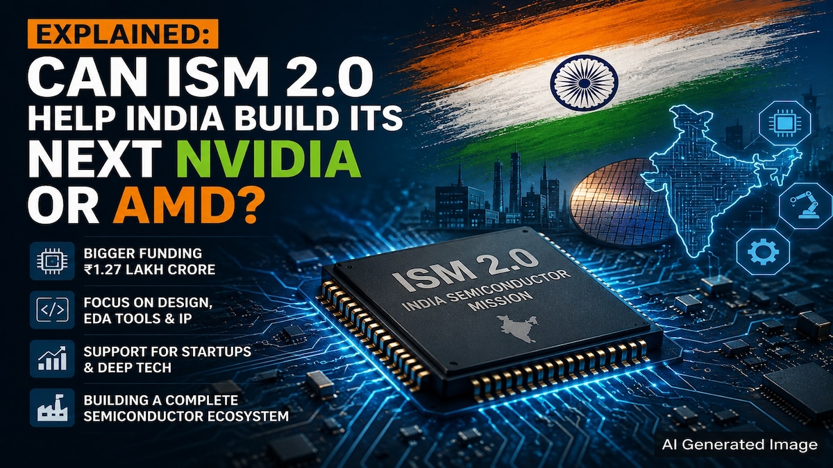
On July 15, the Union Cabinet greenlit the second phase of the India Semiconductor Mission (ISM 2.0), boasting an outlay of ₹1.27 lakh crore — almost 1.7 times the ₹76,000 crore designated for its first phase.
The importance of ISM 2.0 is not just in its financial allocation. The more significant change lies in the mission’s expanded scope.
While the initial phase was primarily centered on enhancing semiconductor manufacturing capacity, the second phase aims for a more comprehensive strategy — encompassing chip design, electronic design automation (EDA) tools, semiconductor equipment, materials, and startups.
This ambition transcends merely producing chips in India.
India’s goal is to establish a complete semiconductor ecosystem — ultimately fostering companies capable of developing globally competitive semiconductor technologies.
This raises a larger query: Can ISM 2.0 pave the way for India to create its next NVIDIA or AMD?
The brief answer is that the initiative, on its own, cannot fabricate a global chip giant. However, it could help dismantle some of the significant structural challenges that have historically impeded the growth of semiconductor firms in India.
Why is ISM 2.0 essential?
The semiconductor push in India commenced with ISM’s first phase, launched in 2021, when the government aimed to build domestic semiconductor production and design capabilities.
The initial emphasis was understandably on establishing the physical infrastructure vital for the sector. Semiconductor fabrication plants require billions in investment and specialized facilities.
However, a robust semiconductor industry can’t thrive on fabs alone.
It also necessitates chip designers, intellectual property providers, equipment manufacturers, materials suppliers, testing and packaging firms, engineering talent, and startups capable of developing new technologies.
That’s where the second phase is anticipated to diverge.
As noted by Rajan Anandan, MD of Peak XV Partners, India had almost no semiconductor startup ecosystem six years ago. Today, there are over 40 funded fabless semiconductor companies in the country.
“Six years ago, India lacked a semiconductor industry. Now, we’re on the path to actually establishing one,” Anandan shared in an interview with CNBC-TV18.
The ecosystem is rapidly evolving across various segments of the value chain, from fabless chip design to fabrication and semiconductor equipment.
The government foresees ISM 2.0 attracting nearly ₹4 lakh crore in investments over a 10 to 12-year period. It’s also projected to generate semiconductor production valued at around ₹2 lakh crore and exports near ₹1 lakh crore throughout its duration.
Thus, the focus is shifting from merely establishing semiconductor factories to cultivating semiconductor capabilities.
How does ISM 2.0 differ from the initial phase?
The first phase was primarily about laying the groundwork for semiconductor production in India.
The second phase is set to widen that approach.
This difference can be summarized as follows:
- ISM 1.0: Establish manufacturing capacity and attract significant semiconductor projects.
- ISM 2.0: Develop a broader ecosystem encompassing design, equipment, materials, intellectual property, and startups.
This distinction is relevant because the semiconductor industry isn’t a monolithic entity.
A company can design a chip without having to manufacture it. Conversely, another firm can handle the manufacturing of chips designed elsewhere. Additionally, there are companies supplying the necessary equipment, materials, and software for both.
For India to become a viable semiconductor hub, it must engage with the entire value chain.
For startups, the structure of support could be as crucial as the magnitude of financial investment.
The government is anticipated to offer support for semiconductor design, including access to costly EDA tools, and may consider co-investment support, allowing public funds to be invested alongside private investors.
Both initiatives could alleviate significant hurdles faced by early-stage semiconductor enterprises.
Why are EDA tools crucial?
A semiconductor is conceptualized long before it is produced.
Engineers require specialized software to develop chip architectures, simulate functionality, verify designs, and catch errors before any manufacturing takes place.
These tools are known as electronic design automation, or EDA, tools.
The cost of these tools can be extraordinarily high, particularly for startups with limited revenue focused on developing their initial products.
Shashwath TR, Co-Founder of Mindgrove Technologies, stated that access to EDA tools has been pivotal in enabling the company to advance its semiconductor technology.
“Mindgrove wouldn’t exist today without that EDA tool support,” he expressed.
For early-stage firms, government backing for EDA tools can lessen the capital needed for fundamental infrastructure.
This enables startups to allocate a greater portion of their funds toward engineering, product development, testing, and commercialization.
Support in obtaining intellectual property and specialized expertise could also be significant.
A chip company doesn’t have to innovate every component of a design from the ground up. It can license specific technology blocks, or IP, while concentrating on areas that provide its competitive edge.
Lowering the costs associated with accessing these tools and resources could help more Indian semiconductor startups transition from concept to market-ready products.
Why might government co-investment be beneficial?
Semiconductor startups are capital-intensive ventures.
The expenses tied to designing, testing, and producing a chip can be substantial, even before a company starts generating significant revenue. Consequently, startups often need to undergo multiple funding rounds over several years.
This creates a financial challenge.
Venture capitalists may be willing to fund early-stage design firms, but the financial requirements to develop semiconductor technologies can far exceed those for many software startups.
This is where government-supported co-investment could play a vital role.
However, the design of such support is crucial.
Dheemanth Nagaraj, Co-Founder and CEO of Agrani Labs, indicated that government participation could be beneficial, provided it does not compromise the control and independence of the founding team.
“To be competitive globally, we must be using a leading process node,” Nagaraj remarked.
He recommended a mechanism that would enable companies to buy back the government’s stake under favorable conditions, making such arrangements more appealing to founders.
This concern is valid. A government stake can impact future fundraising, ownership, governance, and decision-making processes.
Anandan asserted that government co-investment should be seen as an option rather than an obligation.
A startup that opts not to engage with government-backed capital shouldn’t be compelled to do so.
He referenced the Research Development and Innovation (RDI) scheme as a possible model. In that framework, companies could repay a portion of the funding later, all while the government maintains a minor stake.
The overarching principle is straightforward: public investment can help mitigate the early risks associated with establishing semiconductor firms, but it should not supplant private capital or entrepreneurial judgment.
The nuances will ultimately determine whether this model is successful.
Why is the fabless model significant?
One of the most effective ways for India to forge globally competitive semiconductor companies is through the fabless model.
A fabless company focuses on chip design while outsourcing manufacturing to semiconductor foundries.
This enables the firm to concentrate on chip architecture, intellectual property, and product development without needing to construct and run its own fabrication facility.
NVIDIA and AMD exemplify companies that primarily operate under this model.
This approach is crucial since India doesn’t have to establish a fabrication plant for every successful semiconductor enterprise.
A startup might design a chip in India, manufacture it via a global foundry, and sell the finished product to clients worldwide.
Yet, a thriving fabless semiconductor firm requires more than just engineers.
It necessitates access to EDA tools, intellectual property, capital, advanced manufacturing capabilities, testing and packaging facilities, and customers eager to adopt its products.
This illustrates why having a comprehensive ecosystem is indispensable.
The more these resources are available to Indian firms, the fewer obstacles there will be in creating globally competitive semiconductor offerings.
Why do leading-edge process nodes matter?
Simply having capital and talent won’t suffice to establish a global semiconductor powerhouse.
The technology deployed in chip manufacturing is equally vital.
Agrani Labs is working on a GPU targeting the global artificial intelligence market. Nagaraj emphasized that access to advanced manufacturing technology will be crucial for the company’s aspirations.
“To be competitive globally, we must utilize a leading process node,” he stated.
Leading-edge process nodes permit manufacturers to create smaller, more powerful, and energy-efficient chips.
However, achieving these capabilities is remarkably challenging and costly.
The most cutting-edge semiconductor manufacturing technologies are concentrated among a select few companies and nations, including Taiwan, South Korea, and the United States.
India is trying to build its domestic semiconductor manufacturing landscape, but reaching the forefront of process technology will take time.
Nagaraj mentioned that India’s state-of-the-art chips may initially need to be produced through global foundry partners like TSMC or Intel.
However, as India’s fabrication and semiconductor materials ecosystem grows, it could gradually enhance the nation’s domestic capabilities.
This transformation is unlikely to be an instant outcome of ISM 2.0.
Establishing leading-edge semiconductor manufacturing involves years of investment, technological advancement, and operational expertise.
Does India possess the talent to create global chip firms?
Capital and infrastructure alone will not suffice.
The semiconductor sector demands highly specialized engineers, including chip designers, verification engineers, and experts in areas like artificial intelligence hardware.
Anandan indicated that around 20% of the world’s semiconductor designers reside in India.
The challenge is that many of these engineers currently work for global corporations such as NVIDIA, Intel, and AMD.
The opportunity for India lies in motivating more of this talent to establish companies domestically.
Anandan noted that experienced engineers are increasingly departing global tech firms to launch startups in India.
A similar trend is occurring within academic institutions.
Mindgrove was founded by individuals connected to IIT Madras, while the IIT Madras Research Park has emerged as a key hub for deep tech startups.
This exodus of talent from multinational corporations and academic settings into startups could be among the most consequential outcomes of India’s semiconductor initiative.
A nation cannot create a global semiconductor company simply by having engineers.
Yet, it is improbable to build one without them.
Can ISM 2.0 give rise to India’s next NVIDIA or AMD?
NVIDIA and AMD were cultivated over decades. Their competitive advantages reach far beyond just chip design.
They include semiconductor architecture, intellectual property, software ecosystems, developer platforms, access to cutting-edge manufacturing, significant research and development budgets, and strong customer relationships.
Government backing can’t replicate all these capabilities overnight.
ISM 2.0 also can’t assure that a particular Indian startup will emerge as a global technology frontrunner.
Anandan remarked that ISM 2.0 could expedite the development of various segments within the semiconductor value chain, including equipment.
“The momentum has begun. Indian deep tech is in its nascent stages, but we can’t be more enthusiastic about both the talent and the ecosystem,” he declared.
This might be the most pivotal lens through which to view the second phase of India’s semiconductor mission.
ISM 2.0 cannot independently generate India’s next NVIDIA or AMD. Yet, it could help foster the conditions necessary for such companies to be founded, funded, developed, and scaled within India.
Thus, the immediate aim is not to replicate an enterprise that took decades to establish.
Instead, it is to ensure that the forthcoming generation of Indian semiconductor startups has access to tools, capital, talent, infrastructure, and manufacturing collaborations to compete effectively on a global scale.
They could be conceptualized, headquartered, and built right in India.
Why is the broader electronics ecosystem also crucial?
The semiconductor initiative is being complemented by a larger endeavor to enhance electronics manufacturing.
The Union Cabinet has given the go-ahead for a ₹62,500 crore mobile manufacturing scheme for a five-year term. This scheme is projected to generate nearly ₹39 lakh crore in mobile phone production, boost exports, and create around 60,000 direct jobs.
This is important as semiconductors do not thrive in isolation.
An expansive electronics ecosystem creates potential customers, suppliers, and manufacturing allies for semiconductor enterprises.
The combination of semiconductor support and mobile manufacturing incentives is therefore aimed at establishing a comprehensive chain — from chip design and components to production and exports.
For India, the overarching goal is to transition away from merely being a major consumer and assembler of technology products.
The challenge is to evolve into a nation where advanced technologies are also designed, developed, and brought to market.
ISM 2.0 is an attempt to create the infrastructure and financial backing for that shift.
Whether it produces India’s next NVIDIA or AMD will hinge on which companies, technologies, and entrepreneurs emerge over the upcoming decade.
Nonetheless, the policy shift is unambiguous: India is no longer solely attempting to draw semiconductor factories. It is striving to cultivate the ecosystem from which globally competitive semiconductor companies can arise.