The cost benefits may stem from a blend of government incentives that lower capital expenditures, reduced labor costs, competitive electricity tariffs, and the establishment of a domestic supply chain for semiconductor materials, gases, and equipment.
“Considering all these factors, the cost savings could range from over 10% compared to their existing locations,” Sinha remarked.
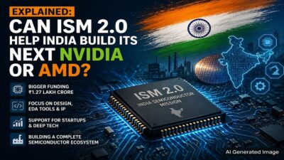
His remarks follow the Union Cabinet’s approval of the second phase of the India Semiconductor Mission (ISM 2.0), which has a budget of ₹1.27 lakh crore. This initiative is projected to span 10 to 12 years, attracting nearly ₹4 lakh crore in investments, generating about ₹2 lakh crore in semiconductor production, and driving exports close to ₹1 lakh crore throughout its duration.
Government incentives to ease capex pressures
Sinha noted that incentives at both the central and state levels would significantly alleviate the capital expenditure burdens for companies establishing semiconductor facilities in India.
“50-60% of their capital expenditures will be depreciated because of this government incentive,” he explained.
According to Sinha, this advantage could empower new semiconductor facilities in India to compete with well-established plants across the globe that have already amortized their initial investments.
Thus, India could present companies with a comparable cost structure, despite being a relatively new player in semiconductor manufacturing, he added.
Reduced operating expenses can enhance India’s competitiveness
The cost advantage may extend beyond the initial facility investments.
Labor and electricity are critical operating expenses in the semiconductor manufacturing process. Sinha indicated that labor accounts for approximately 13% of costs in a fab, while electricity constitutes about 17%.
India’s lower labor costs and the competitive electricity rates provided by state governments could yield additional savings for companies, he noted.
This advantage could be amplified as various parts of the semiconductor supply chain are developed domestically.
“If we can manufacture chemical gases and materials, and if equipment companies engage in R&D and some manufacturing while establishing their support systems in India, this will further reduce operational costs,” Sinha commented.
ISM 2.0 to facilitate government co-investment in semiconductor startups
ISM 2.0 will continue to support semiconductor startups established during the first phase of the initiative, providing seed funding and access to electronic design automation (EDA) tools.
These tools assist chip designers in developing and testing semiconductor designs.
Sinha emphasized that such support helps startups navigate some of the most significant challenges during their early developmental stages. Once a startup creates a proof of concept (POC), it can approach venture capitalists and other investors for funding.
A notable addition in ISM 2.0 is the provision for government co-investment alongside private investors.
“If investors endorse ISM’s decision that a company is promising, [the government] will match the investment under the same terms and conditions as the venture capitalists or investors,” Sinha noted.
This provision was not part of the initial program and could encourage more venture capital into India’s semiconductor startup ecosystem.
Government will not intervene in daily operations
Sinha clarified that the government does not intend to become a hindrance for the startups receiving assistance under the initiative.
While details regarding equity participation, management control, and board representation will be specified in the forthcoming guidelines, he assured that the government would not interfere with the daily operations of companies.
“We are here to support them and not to be seen as a burden on any startup,” Sinha stated.
ISM 2.0 broadens India’s semiconductor aspirations
The second phase of the India Semiconductor Mission represents a more comprehensive strategy than its predecessor, with the government aiming to create an all-encompassing semiconductor ecosystem in India.
While ISM 1.0 heavily concentrated on establishing semiconductor fabrication and packaging capabilities, the new phase is predicted to support a broader array of activities, encompassing semiconductor design, materials, equipment, and other segments of the supply chain.
The Union Cabinet has also given the green light to a separate ₹62,500 crore mobile manufacturing initiative for five years. This scheme is anticipated to foster mobile phone production valued at nearly ₹39 lakh crore and create about 60,000 direct jobs.
Both ISM 2.0 and the mobile manufacturing initiative are expected to be announced within 20 days, as indicated by Electronics and IT Minister Ashwini Vaishnaw.
Watch the accompanying video for the full interview.